Products

SP-7 based Data Acquisition Probe/ SP-7 based Development Board

Overview

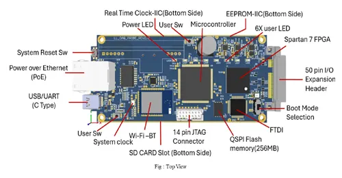
Data Acquisition Probe(DAP)/Development Board is a low cost, compact size solution for moderate speed data acquisition and development of many applications. It supports high performance reconfigurable system with onboard FPGA and microcontroller. The board facilitates high speed inter communication interfaces between FPGA and microcontroller for data processing and control logic. This board has facility to communicate with cloud through onboard Wifi/BT module and custom GUI with USB. It also supports for dedicated applications like Rotary Encoder Test Jig, CAN-FD based DAP or Multichannel Temperature Sensor interface with plug and play adapter board.

Technical Features

  • Power: Multiple options (Expansion Header, USB, PoE).
  • Clocking: 50MHz Crystal, 60MHz FTDI Clock.
  • Communication & Networking: Gigabit Ethernet, USB, Wi-Fi/Bluetooth.
  • Expansion: 2 SPI Masters, 4 CANFD channels, 8 Differential I/Os, Debug UART, GPIO, Power Pins.
  • Processing: Spartan 7 FPGA, Microcontroller.
  • Memory: SD Card (up to 64Mb), 32kb EEPROM, 256Mb Quad SPI Flash.
  • Control & I/O: 6 LEDs, Power Indicator, User Switches.
  • Analog: Voltage/Current Measurement, Onboard configuration circuitry.
  • Inter-Communication: High-Speed EBI, I2C, GPIO.
  • Timing: RTC via I2C.

Linkedloops Zynq 7000 SoC System On Module (SoM)

Overview

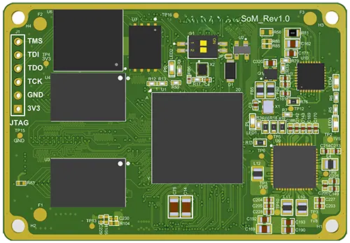
Linkedloops Zynq 7000 SoC SoM is a high-performance System-On-Module (SoM) designed around the Xilinx Zynq- 7000 XC7Z020CLG400-1 SoC, providing a versatile solution for a wide range of embedded applications. With the integration of both dual-core ARM Cortex-A9 processors and FPGA fabric, this module delivers the best of both software programmability and hardware acceleration. The SoM is designed with scalability in mind, allowing migration between Zynq-7000 series devices, such as the XC7Z010, XC7Z015, XC7Z020, and XC7Z030, in a pin-compatible layout for maximum flexibility. The SoM is plug-in module for any custom carrier board, reducing board design cycle time and complexity.

Technical Features

  • SoC Options: XC7Z010, XC7Z015, XC7Z020, XC7Z030 with pin-compatible Zynq SoCs for scalability.
  • Memory: DDR3 SDRAM (1GB, expandable).
  • 16GB eMMC Flash for storage.
  • 32MB/64MB QSPI Flash for fast boot.
  • Connectivity: USB 2.0 PHY, up to 148 user I/O (113 for XC7Z010)
  • Power Management: High-efficiency PMIC, dynamic power modes.
  • PCB Specs:
    Size: 65mm x 45mm.
    Two 100-pin SMD high-speed connectors.
    Clocks and Timing: 33.33 MHz oscillator, programmable PLLs.
    Thermal Management: Heatsink mounting support for effective cooling.
    Boot/Reset Options: QSPI/JTAG boot, reliable reset circuit.

CANFD

CANFD based Data-Logger

Overview

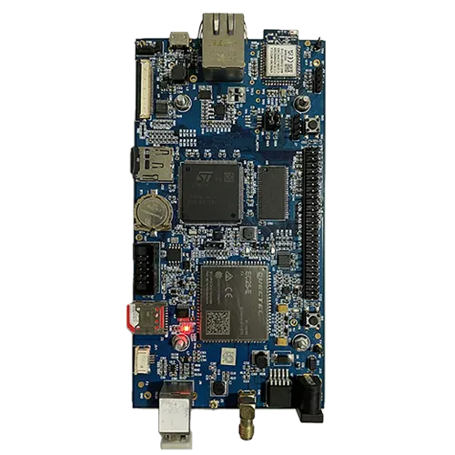
The CANFD based Data-Logger by Linkedloops Intelligence is an in-vehicle data logger tailored for engineering and diagnostics. Designed as a rugged, feature-rich device, CANFD based Data-Logger supports advanced data acquisition for vehicle fleet monitoring and network data logging applications. This indigenous Indian solution offers reliable performance in extreme conditions, with capabilities to log data without frame loss, conduct remote diagnostics, and perform wireless data transfers. Integrated with Linkedloops MTS, CANFD based Data-Logger enables remote device management, data analytics, and real-time monitoring.

Technical Details

  • Channels and Interfaces: 4 CAN / CAN-FD channels, DoIP (Diagnostic over IP), Gigabit Ethernet, USB 2.0, Wi-Fi, and GPS.
  • Storage: Micro SD storage options (32 to 128 GB).
  • Precision and Reliability: <50 ns timestamp accuracy, IP66 ruggedness rating, and no frame loss capability.
  • Remote Diagnostics and Configurations: Wireless data transfer and configuration, supported by a dedicated wireless server.
  • Scripting and Trigger Functions: Onboard scripting with start/stop triggers, error-based conditions, and logging options.
  • Input/Output (I/O): 2 analog inputs, 1 digital input, and 1 digital output.
  • Power: 6 – 36V DC input range, power consumption under 5W, with sleep/wake on CANFD capabilities.
  • Environmental Specifications: Operating temperature range of -40°C to 85°C.

IO Controller

Flexible Industrial IO Controller with Gateway Functionality

Overview

The Linkedloops Flexible Industrial IO Controller with Gateway Functionality is a versatile solution for industrial process control and IoT connectivity.

It features configurable digital and analog I/O with robust protections, integrated connectivity options (Ethernet, Wi-Fi, 4G LTE, BLE, and LoRa), and advanced safety mechanisms such as tamper detection and thermal shutdown. Its modular design, rich software configurability, and comprehensive support for protocols like MODBUS make it ideal for diverse industrial applications.

Features

  • Modular design
  • Configurable inputs/outputs
  • GUI – configuration and control
  • Android App – configuration and control
  • MODBUS
  • OTAP
  • BLE 5.0, LoRa
  • Graphic display support – 800 X 480 with touchscreen

Ultra-high Resolution Encoder
Test Jig

Overview

The Ultra-High Resolution Encoder Test Jig is a compact and versatile solution for testing the accuracy and performance of various types of encoders. Designed with a Spartan 7 FPGA for reconfigurability, it features multiple modes of encoder testing, data analysis, and logging capabilities, making it an essential tool for precision encoder evaluation.

Technical Features

  • Compact in size
  • Easy to connect and operate
  • Graphical User Interface (GUI) for monitoring and controlling encoder test process
    USB to support windows PC connection(GUI)
  • Graph based encoder performance analysis
  • Various error detection and indication
  • Capturing and storage of test data in excel sheet for further analysis
  • SPARTAN 7 FPGA based design facilitates
  • Reconfigurability for various encoders
  • Add on microcontroller to manage cloud data logistics
  • On board Wi-Fi interface
  • Multiple powering options – Power supply through IO Header, USB, PoE
  • On-board current and voltage measurement of
  • Encoder signals
  • RTC interface for time stamping

Multi-Channel Temperature Sensor

Overview

Aiming at the high and low temperature test requirements of cars before being sent on roads, this paper designs and implements a multi-channel thermocouple temperature measurement system based on FPGA. The system adopts thermocouple as temperature sensor, and K Type is used as thermocouple cold junction temperature compensation, which solves the problem of thermocouple cold junction compensation better. The front end adopts MAX11200, a 24-bit analog-to-digital converter with low noise, multi-channel and low power consumption, to amplify and A/D convert the signal at measuring junction of thermocouple. The control core is a field programmable logic gate array FPGA, which can better solve the problem of parallel processing of multi-channel temperature signals. At the same time, it uses the transposition method of the thermocouple standard graduation table, the interpolation look-up table algorithm and the cold junction compensation reverse look-up table algorithm, which is effective. The temperature measurement accuracy of each channel is improved. The experimental results show that the system can be connected to 8 K-type thermocouple sensors, the measurement range can reach -200℃~220℃ (73.15K~493.15K), and the relative error is less than ±0.3%F.S.

Technical Features

  • FPGA Mach XO2 7000 with Flash Memory , Plug and Play model.
  • 8 channel compatible for each board.
  • 23 bits ENOB (Effective Number of Bits) for each Temperature Channel with ADC MAX11200 which is ultra low-power (< 300FA active current), high-resolution, serial output.
  • 201 bit FRAME, where 192 bits is 8 channel ADC data, 6 bits are Device ID, and 3 bits are CRC bits (Cyclic Redundancy Check) for error detection.
  • K Type Thermocouple with temperature range 200℃~220℃.
  • Parallel multiplexing and data processing at 50Mhz speed.
  • ADC conversion time ~ 10usec with 10 SPS (Samples Per Seconds) settings.
  • LVDS connections between MTS board for longer connectivity and noise elimination.
  • On Board Op-to Couplers for device protection.
  • USB, Ethernet, Wi-Fi and SD card compatibility for data outsourcing

LPROG

USB-JTAG XILINX FPGA PROGRAMMER

Overview

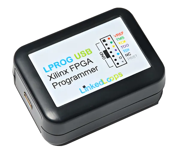
LPROG is a compact, low cost programmer for Xilinx FPGA devices. LPROG connects to USB port on a host machine using USB C type cable. It connects to LPROG programmer using USB C type cable. The LPROG derives 5V supply from host USB port for internal circuit operation. No external power supply is needed. LPROG connects to target system using a 14 pin ribbon cable with standard JTAG interface.
LPROG takes VREF supply input from JTAG port for IO voltage compatibility. VREF can vary from 1.8V to 5V. JTAG port also has a soft reset pin which is used to reset the processor core of Zynq series FPGA devices.
A 14 pin, 2mm pitch box header from Molex is expected to be used on FPGA device platforms for FRC cable compatibility. Alternately flying leads are provided for non-standard connections of Compatible JTAG programming connector.

Features

  • USB host connectivity
  • 14 pin standard JTAG connector
  • 1.8V to 5V JTAG interface
  • A Soft Reset pin support (Zynq Devices)
  • Compatibility with Xilinx tools

Overview

The Wireless Lora Switch is an innovative solution that allows you to effortlessly control your AC appliances using Lora wireless technology. This device operates on a 5V DC power supply and offers seamless and convenient control over your devices. With the power of Lora wireless technology, you can now control your AC appliances from anywhere within 1KM. Whether you’re at distant location, the Wireless Lora Switch enables you to conveniently turn on or off your devices with a Switch.

Features

  • Wireless Communication: The switch supports wireless communication with a range of up to 1KM using LoRa technology.
  • Battery Operated: It can be operated on a rechargeable battery, making it fully battery-operated. The board includes a battery charger to charge the battery. Battery life is 6 to 8 hrs.
  • User Interface: The switch has three user-friendly touch sensors for control. There are three LED’s for status indication for switch and one LED for battery voltage indication.
  • AC Device Control: The switch is designed to control AC devices such as bulbs, motors,pumps etc. It can be used as a single-phase or 3-phase AC device switch.
  • Power Path Management: The system has power path management to optimize charging from weak adapters while powering the system.
  • Frequency range: 868 MHz
  • Power Supply: Lora Driver operates on AC supply. Lora Switch operates on battery which takes 5v dc for charging through USB type C cable.
  • Switch Outputs: It provides three-channel switch outputs for controlling appliances. The rated output voltage for AC is 220 to 250v at 50/60Hz.
  • Connection Blocks: The output terminals are connected with Push-in termination blocks, providing convenience for connecting and disconnecting appliances.
  • Easy Communication: LoRa technology provides long-range communication without requiring cellular or Wi-Fi networks
  • Operation: The switch is designed to operate three appliances simultaneously.

Schedule A Call

Thanks for expressing your interest in our products. Please fill out the form below, and we will be in touch shortly.

Preferred Date and Time to Contact